Specific Materials Examples
This document provides a comprehensive catalog of materials science tutorials organized by the MCODE (Materials Categorization by Ontology, Dimensionality and Evolution) system. Each entry includes:
- Structure Notebook: Creates the atomic structure from published manuscripts
- Properties Notebook: Calculates and reproduces key properties from the manuscript
- DOI Reference: Link to the original scientific publication
1. Pristine Structures
1.1. 2D Structures
1.1.1. Slab
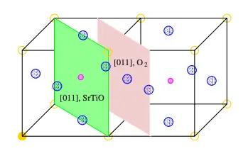
1.1.1.1. SrTiO3 Slab P-2D-SLB-S
Structure: Create SrTiO3 Slab Structure
Properties: Calculate Surface Energies of SrTiO3(011) and (001) Terminations
DOI: 10.1103/PhysRevB.77.195408 12
1.2. 0D Structures
1.2.1. Nanoparticle
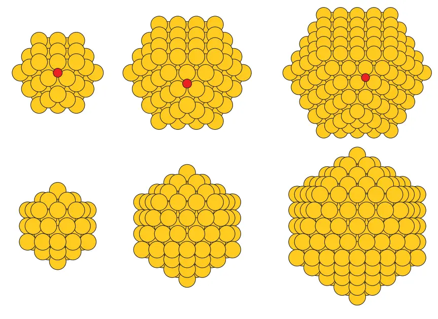
1.2.1.1. Gold Nanoclusters P-0D-NPR
Structure: Create Gold Nanocluster Structure
Properties: Calculate total energy per atom and density of states (Coming Soon)
DOI: 10.1103/PhysRevB.84.245429 3
2. Compound Pristine Structures
2.1. 2D Structures
2.1.1. Interface
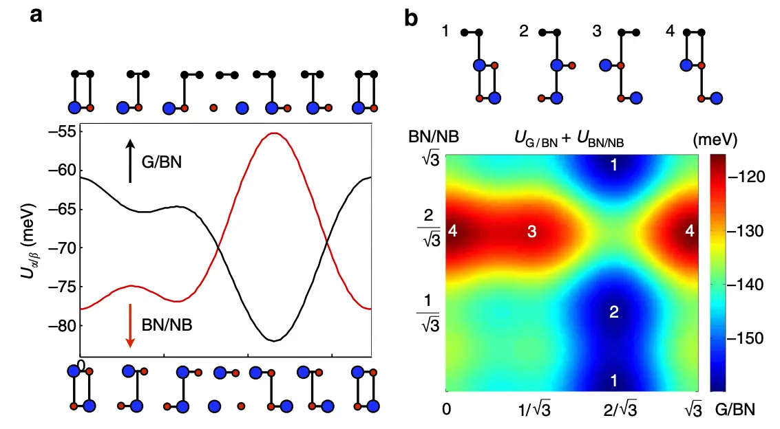
2.1.1.1. Graphene/h-BN Interface C-2D-INT-Z
Structure: Create Graphene/h-BN Interface
Properties: Calculate Stacking Energy and Band Gap of Graphene on h-BN
DOI: 10.1038/ncomms7308 4
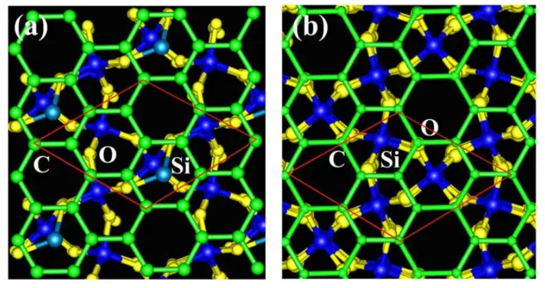
2.1.1.2. Graphene/SiO2 Interface C-2D-INT-Z
Structure: Create Graphene/SiO2 Interface
Properties: Calculate Doping and Gap at the Dirac Point of Graphene on SiO2
DOI: 10.1103/PhysRevB.78.115404 5
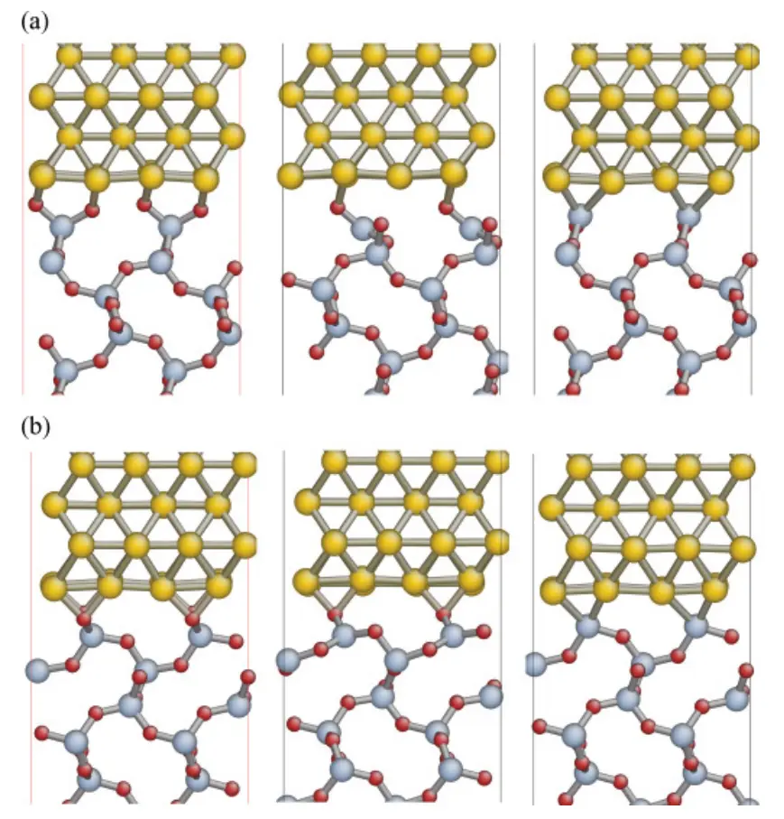
2.1.1.3. Copper/SiO2 Interface C-2D-INT-Z
Structure: Create Copper/Cristobalite Interface
Properties: Calculate band structure (Coming Soon)
DOI: 10.1103/PhysRevB.83.115327 6
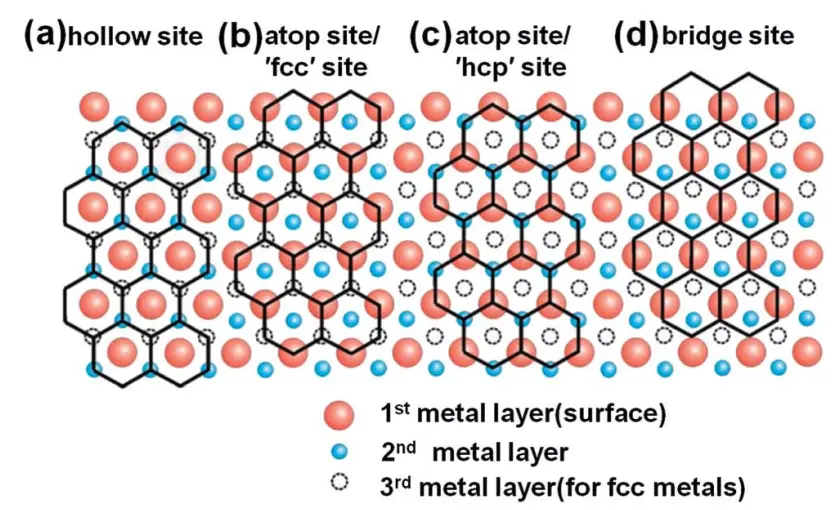
2.1.1.4. Graphene/Ni(111) Interface Optimization C-2D-INT-Z
Structure: Create Graphene/Ni(111) Interface
Properties: Calculate total energies versus lateral shift and band structure (Coming Soon)
DOI: 10.1039/c3nr05279f 789
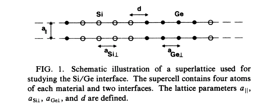
2.1.1.5. Si/Ge (001) Interface C-2D-INT-S
Structure: Create Si/Ge (001) Interface
Properties: Calculate Si/Ge (001) Valence Band Offset
DOI: 10.1103/PhysRevB.34.5621 10
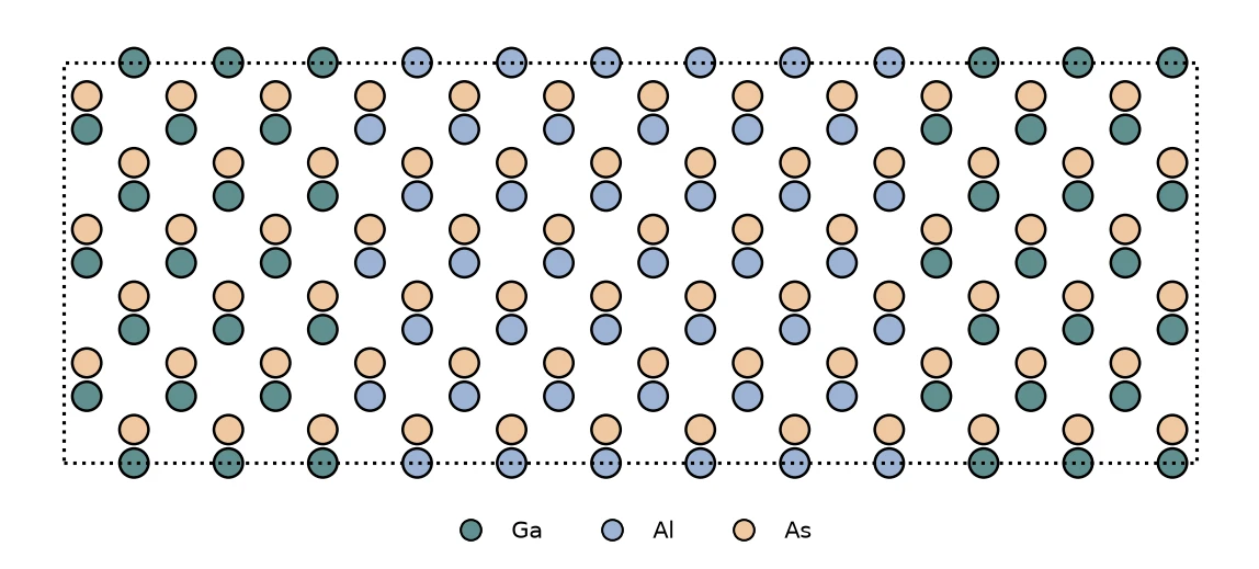
2.1.1.6. GaAs/AlAs (110) Interface C-2D-INT-S
Structure: Create GaAs/AlAs (110) Interface
Properties: Calculate GaAs/AlAs (110) Valence Band Offset
DOI: 10.1103/PhysRevB.90.155405 11
2.1.2. Heterostack
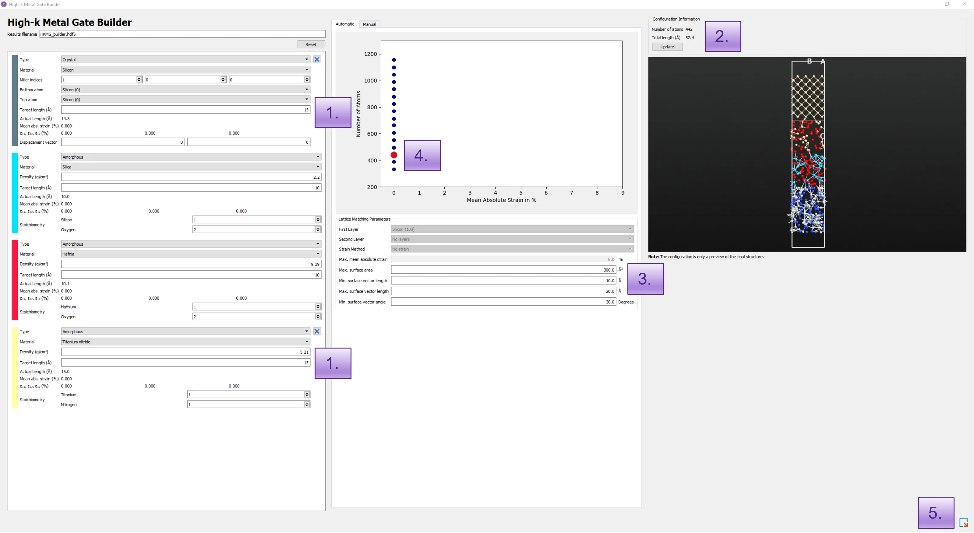
2.1.2.1. High-k Metal Gate Stack (Si/SiO2/HfO2/TiN) C-2D-HST
Structure: Create High-k Metal Gate Stack
Properties: Calculate band structure and valence band offset (Coming Soon)
Reference: QuantumATK Tutorial 1213
2.1.3. Interface - Twisted
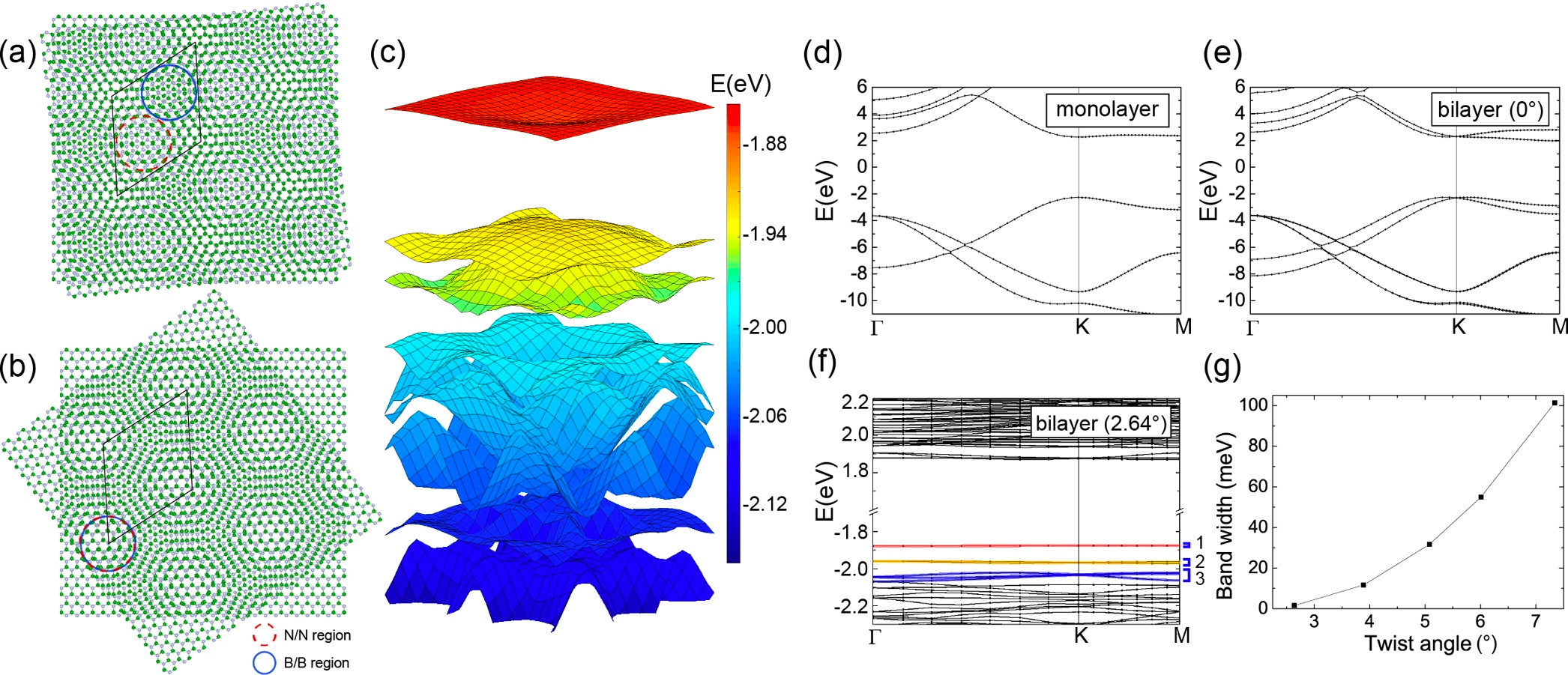
2.1.3.1. Twisted Bilayer h-BN Nanoribbons C-2D-INT-T
Structure: Create Twisted h-BN Nanoribbons
Properties: Calculate band structure and total energies versus twist angle (Coming Soon)
DOI: 10.1021/acs.nanolett.9b00986 14
2.1.4. Interface - Commensurate
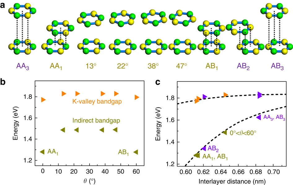
2.1.4.1. Twisted Bilayer MoS2 Commensurate Lattices C-2D-INT-C
Structure: Create Twisted MoS2 Commensurate Lattices
Properties: Calculate Band Structure of Twisted MoS2 Bilayers
DOI: 10.1038/ncomms5966 1516
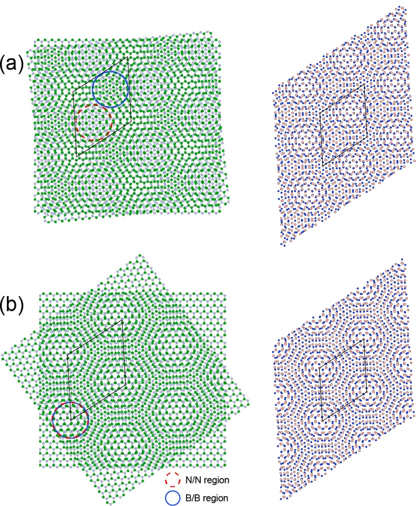
2.1.4.2. Twisted Bilayer h-BN Commensurate Lattices C-2D-INT-C
Structure: Create Twisted h-BN Commensurate Lattices
Properties: Calculate Flat Bands of Twisted Bilayer h-BN
DOI: 10.1021/acs.nanolett.9b00986 14
3. Defective Structures
3.1. 2D Structures
3.1.1. Island
3.1.1.1. Island Surface Defect Formation in TiN D-2D-ISL
Structure: Create Island Defect on TiN Surface
Properties: Calculate island formation energy (Coming Soon)
DOI: 10.1103/PhysRevB.97.035406 17
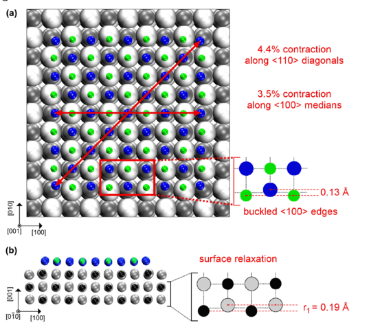
3.1.1.2. Pt Adatoms Island on MoS2 D-2D-ISL
Structure: Create Pt Island on MoS2
Properties: Calculate Binding Energy per Pt Atom on MoS2
DOI: 10.1021/cg5013395 1819202122
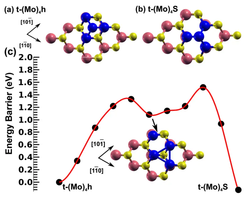
3.1.2. Terrace
3.1.2.1. Step Surface Defect on Pt(111) D-2D-TER
Structure: Create Step Defect on Pt(111)
Properties: Calculate O₂ Dissociation Barrier on Pt(111) and at the Pt(211) Step
DOI: 10.1016/s0039-6028(02)01908-8 23
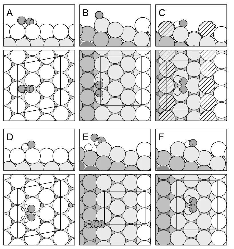
3.1.3. Adatom
3.1.3.1. Adatom Surface Defects on Graphene D-2D-ADA
Structure: Create Adatom Defects on Graphene
Properties: Calculate adsorption energy, density of states, work function, dipole moment, and diffusion barriers (Coming Soon)
DOI: 10.1103/PhysRevB.77.235430 24
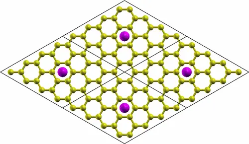
3.1.4. Grain Boundary Planar
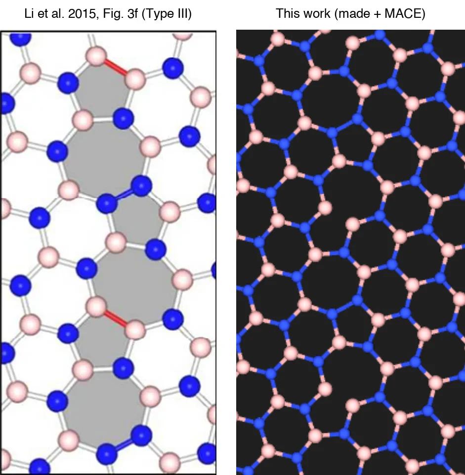
3.1.4.1. Grain Boundary in h-BN D-2D-GBP
Structure: Create Grain Boundary in h-BN
Properties: Calculate Band Gap and LDOS at the Grain Boundary in h-BN
DOI: 10.1021/acs.nanolett.5b01852 25
3.2. 1D Structures
3.2.1. Grain Boundary Linear
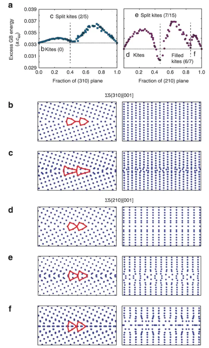
3.2.1.1. Grain Boundary in FCC Metals (Copper) D-1D-GBL
Structure: Create Grain Boundary in Copper
Properties: Calculate defect energy per atom (Coming Soon)
DOI: 10.1038/ncomms2919 26
3.3. 0D Structures
3.3.1. Substitution
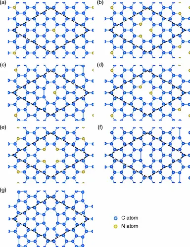
3.3.1.1. Substitutional Point Defects in Graphene D-0D-SUB
Structure: Create Substitutional Defects in Graphene
Properties: Calculate Band Structure of N-doped Graphene
DOI: 10.1103/PhysRevB.84.245446 27
3.3.2. Defect Pair
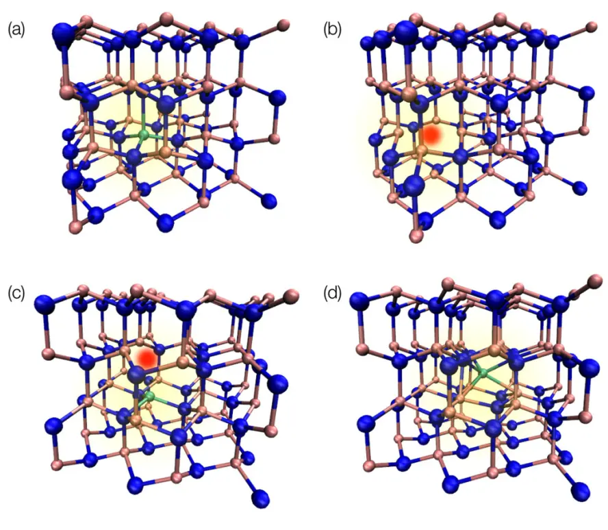
3.3.2.1. Vacancy-Substitution Pair Defects in GaN D-0D-DFP
Structure: Create Vacancy-Substitution Pair in GaN
Properties: Calculate Formation Energy of the Mg_Ga-V_N Pair in GaN
DOI: 10.1103/PhysRevB.93.165207 28
3.3.3. Vacancy
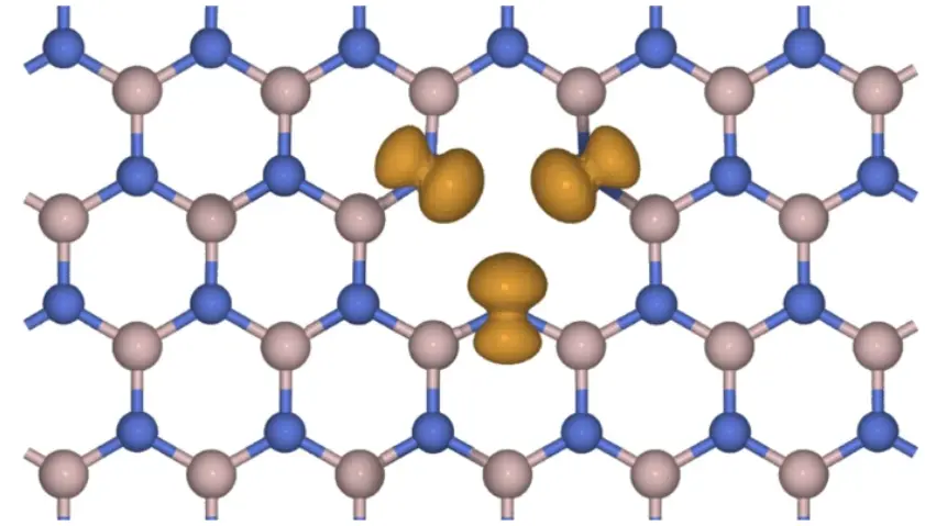
3.3.3.1. Vacancy Point Defect in h-BN D-0D-VAC
Structure: Create Vacancy Defect in h-BN
Properties: Calculate Formation Energy of a Boron Vacancy in h-BN
DOI: 10.1038/s41524-022-00730-w 29
3.3.4. Interstitial
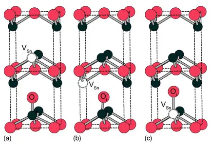
3.3.4.1. Interstitial Point Defect in SnO D-0D-INT
Structure: Create Interstitial Defect in SnO
Properties: Calculate Formation Energy and Density of States of the V_Sn-O_i Pair in SnO
DOI: 10.1103/PhysRevB.74.195128 303132
4. Processed Structures
4.1. 3D Structures
4.1.1. Perturbation
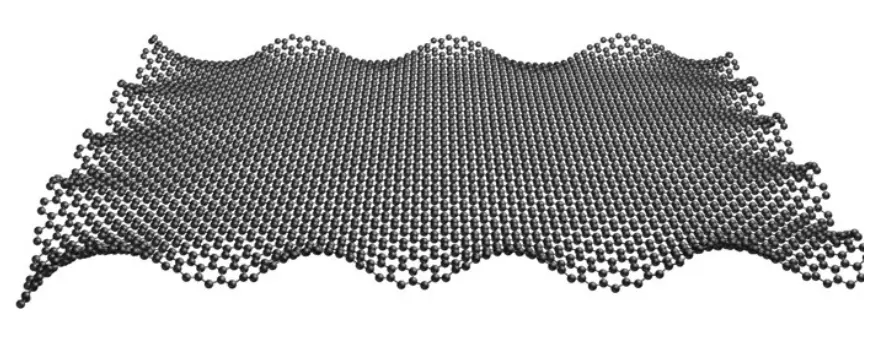
4.1.1.1. Ripple Perturbation of Graphene Sheet X-3D-PER
Structure: Create Rippled Graphene Structure
DOI: 10.1209/0295-5075/85/46002 333435
4.2. 2D Structures
4.2.1. Passivated Surface
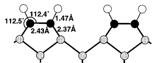
4.2.1.1. H-Passivated Silicon (100) Surface X-2D-PAS
Structure: Create H-Passivated Si(100) Surface
Properties: Calculate H and D diffusion barriers, reaction and desorption barriers (Coming Soon)
DOI: 10.1103/PhysRevB.57.13295 363738
4.3. 1D Structures
4.3.1. Passivated Edge
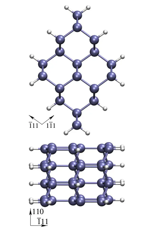
4.3.1.1. H-Passivated Silicon Nanowire X-1D-PAS
Structure: Create H-Passivated Si Nanowire
Properties: Calculate band gap, density of states, and formation energy (Coming Soon)
DOI: 10.1103/PhysRevB.76.035305 39
References
-
R. I. Eglitis and David Vanderbilt. First-principles calculations of atomic and electronic structure of srtio3 (001) and (011) surfaces. Phys. Rev. B, 77:195408, May 2008. URL: https://link.aps.org/doi/10.1103/PhysRevB.77.195408. ↩
-
Atashi B. Mukhopadhyay, Javier F. Sanz, and Charles B. Musgrave. First-principles calculations of structural and electronic properties of monoclinic hafnia surfaces. Phys. Rev. B, 73:115330, Mar 2006. URL: https://link.aps.org/doi/10.1103/PhysRevB.73.115330. ↩
-
Ask Hjorth Larsen, Jesper Kleis, Kristian Sommer Thygesen, Jens K. Nørskov, and Karsten Wedel Jacobsen. Electronic shell structure and chemisorption on gold nanoparticles. Phys. Rev. B, 84(24):245429, 2011. URL: https://doi.org/10.1103/PhysRevB.84.245429. ↩
-
Jeil Jung, Ashley M. DaSilva, Allan H. MacDonald, and Shaffique Adam. Origin of band gaps in graphene on hexagonal boron nitride. Nature Communications, 6:6308, 2015. URL: https://doi.org/10.1038/ncomms7308. ↩
-
Yong-Ju Kang, Joongoo Kang, and K. J. Chang. Electronic structure of graphene and doping effect on sio2. Physical Review B, 78:115404, 2008. URL: https://link.aps.org/doi/10.1103/PhysRevB.78.115404. ↩
-
T.-R. Shan, B. D. Devine, S. R. Phillpot, and S. B. Sinnott. Molecular dynamics study of the adhesion of cu/sio2 interfaces using a variable-charge interatomic potential. Physical Review B, 83(11):115327, 2011. URL: https://doi.org/10.1103/PhysRevB.83.115327. ↩
-
Arjun Dahal and Matthias Batzill. Graphene–nickel interfaces: a review. Nanoscale, 6:2548–2562, 2014. URL: https://doi.org/10.1039/C3NR05279F. ↩
-
Y. Gamo, A. Nagashima, M. Wakabayashi, M. Terai, and C. Oshima. Atomic structure of monolayer graphite formed on ni(111). Surface Science, 374(1-3):61–64, 1997. URL: https://www.sciencedirect.com/science/article/abs/pii/S0039602896007856. ↩
-
G. Bertoni, L. Calmels, A. Altibelli, and V. Serin. First-principles calculation of the electronic structure and eels spectra at the graphene/ni(111) interface. Physical Review B, 71(7):075402, 2005. URL: https://journals.aps.org/prb/abstract/10.1103/PhysRevB.71.075402. ↩
-
Chris G. Van de Walle and Richard M. Martin. Theoretical calculations of heterojunction discontinuities in the Si/Ge system. Physical Review B, 34:5621–5634, 1986. URL: https://link.aps.org/doi/10.1103/PhysRevB.34.5621. ↩
-
Yoyo Hinuma, Andreas Grüneis, Georg Kresse, and Fumiyasu Oba. Band alignment of semiconductors from density-functional theory and many-body perturbation theory. Physical Review B, 90:155405, 2014. URL: https://link.aps.org/doi/10.1103/PhysRevB.90.155405. ↩
-
D. A. Muller, T. Sorsch, S. Moccio, F. H. Baumann, K. Evans-Lutterodt, and G. Timp. The electronic structure at the atomic scale of ultrathin gate oxides. Nature, 399:758–761, 1999. URL: https://doi.org/10.1038/21602. ↩
-
J Robertson. High dielectric constant gate oxides for metal oxide si transistors. Reports on Progress in Physics, 69:327, 2006. URL: https://doi.org/10.1088/0034-4885/69/2/R02. ↩
-
Lede Xian, Dante M. Kennes, Nicolas Tancogne-Dejean, Massimo Altarelli, and Angel Rubio. Multiflat bands and strong correlations in twisted bilayer boron nitride: doping-induced correlated insulator and superconductor. Nano Lett., 19(8):4934–4940, 2019. URL: https://doi.org/10.1021/acs.nanolett.9b00986. ↩↩
-
Kaihui Liu, Liming Zhang, Ting Cao, Chenhao Jin, Diana Qiu, Qin Zhou, Alex Zettl, Peidong Yang, Steve G. Louie, and Feng Wang. Evolution of interlayer coupling in twisted molybdenum disulfide bilayers. Nature Communications, 5:4966, 2014. URL: https://doi.org/10.1038/ncomms5966, doi:10.1038/ncomms5966. ↩
-
Yuan Cao, Valla Fatemi, Shiang Fang, Kenji Watanabe, Takashi Taniguchi, Efthimios Kaxiras, and Pablo Jarillo-Herrero. Unconventional superconductivity in magic-angle graphene superlattices. Nature, 556:43–50, 2018. URL: https://doi.org/10.1038/nature26160. ↩
-
D. G. Sangiovanni, A. B. Mei, D. Edström, L. Hultman, V. Chirita, I. Petrov, and J. E. Greene. Effects of surface vibrations on interlayer mass transport: ab initio molecular dynamics investigation of ti adatom descent pathways and rates from tin/tin(001) islands. Physical Review B, 97:035406, 2018. URL: https://link.aps.org/doi/10.1103/PhysRevB.97.035406. ↩
-
W. A. Saidi. Density functional theory study of nucleation and growth of pt nanoparticles on mos2(001) surface. Crystal Growth & Design, 15(2):642–652, 2015. URL: https://doi.org/10.1021/cg5013395. ↩
-
M. Jiao, W. Song, H.-J. Qian, Y. Wang, Z. Wu, S. Irle, and K. Morokuma. Qm/md studies on graphene growth from small islands on the ni(111) surface. Nanoscale, 8(5):3067–3074, 2016. URL: https://doi.org/10.1039/c5nr07680c. ↩
-
Kristen A. Fichthorn and Matthias Scheffler. Island nucleation in thin-film epitaxy: a first-principles investigation. Phys. Rev. Lett., 84:5371, 2000. URL: https://link.aps.org/doi/10.1103/PhysRevLett.84.5371. ↩
-
Jörg Neugebauer and Matthias Scheffler. Mechanisms of island formation of alkali-metal adsorbates on al(111). Phys. Rev. Lett., 71:577, 1993. URL: https://link.aps.org/doi/10.1103/PhysRevLett.71.577. ↩
-
Mahbube Hortamani, Peter Kratzer, and Matthias Scheffler. Density-functional study of mn monosilicide on the si(111) surface: film formation versus island nucleation. Phys. Rev. B, 76:235426, 2007. URL: https://link.aps.org/doi/10.1103/PhysRevB.76.235426. ↩
-
Ž. Šljivančanin and B. Hammer. Oxygen dissociation at close-packed Pt terraces, Pt steps, and Ag-covered Pt steps studied with density functional theory. Surface Science, 515(1):235–244, 2002. URL: https://doi.org/10.1016/s0039-6028(02)01908-8. ↩
-
Kevin T. Chan, J. B. Neaton, and Marvin L. Cohen. First-principles study of metal adatom adsorption on graphene. Phys. Rev. B, 77:235430, 2008. URL: https://link.aps.org/doi/10.1103/PhysRevB.77.235430. ↩
-
Qiucheng Li, Xiaolong Zou, Mengxi Liu, Jingyu Sun, Yabo Gao, Yue Qi, Xiebo Zhou, Boris I. Yakobson, Yanfeng Zhang, and Zhongfan Liu. Grain boundary structures and electronic properties of hexagonal boron nitride on cu(111). Nano Letters, 15(9):5804–5810, 2015. URL: https://doi.org/10.1021/acs.nanolett.5b01852. ↩
-
Timofey Frolov, David L Olmsted, Mark Asta, and Yuri Mishin. Structural phase transformations in metallic grain boundaries. Nature Communications, 4:1899, 2013. URL: https://doi.org/10.1038/ncomms2919. ↩
-
Yoshitaka Fujimoto and Susumu Saito. Formation, stabilities, and electronic properties of nitrogen defects in graphene. Phys. Rev. B, 84:245446, Dec 2011. URL: https://link.aps.org/doi/10.1103/PhysRevB.84.245446. ↩
-
Giacomo Miceli and Alfredo Pasquarello. Self-compensation due to point defects in mg-doped gan. Physical Review B, 93:165207, 2016. URL: https://link.aps.org/doi/10.1103/PhysRevB.93.165207. ↩
-
Fabian Bertoldo, Sajid Ali, Simone Manti, and Kristian S. Thygesen. Quantum point defects in 2d materials - the qpod database. npj Computational Materials, 8(1):56, 2022. URL: https://doi.org/10.1038/s41524-022-00730-w. ↩
-
A. Togo, F. Oba, I. Tanaka, and K. Tatsumi. First-principles calculations of native defects in tin monoxide. Physical Review B, 74(19):195128, 2006. URL: https://doi.org/10.1103/PhysRevB.74.195128. ↩
-
H. Wang, A. Chroneos, C. A. Londos, E. N. Sgourou, and U. Schwingenschlögl. Carbon related defects in irradiated silicon revisited. Scientific Reports, 4:4909, 2014. URL: https://doi.org/10.1038/srep04909. ↩
-
Sutassana Na-Phattalung, M. F. Smith, Kwiseon Kim, Mao-Hua Du, Su-Huai Wei, S. B. Zhang, and Sukit Limpijumnong. First-principles study of native defects in anatase tio2. Physical Review B, 73:125205, 2006. URL: https://doi.org/10.1103/PhysRevB.73.125205. ↩
-
R. C. Thompson-Flagg, M. J. B. Moura, and M. Marder. Rippling of graphene. EPL (Europhysics Letters), 85(4):46002, 2009. URL: https://doi.org/10.1209/0295-5075/85/46002. ↩
-
A. Fasolino, J. H. Los, and M. I. Katsnelson. Intrinsic ripples in graphene. Nature Materials, 6:858–861, 2007. URL: https://doi.org/10.1038/nmat2011. ↩
-
L. A. Openov and A. I. Podlivaev. Interaction of the stone-wales defects in graphene. Physics of the Solid State, 57(7):1477–1481, 2015. URL: https://doi.org/10.1134/S1063783415070240. ↩
-
U. Hansen and P. Vogl. Hydrogen passivation of silicon surfaces: a classical molecular-dynamics study. Physical Review B, 57(20):13295–13304, 1998. URL: https://doi.org/10.1103/physrevb.57.13295. ↩
-
J. E. Northrup. Structure of si(100)h: dependence on the h chemical potential. Physical Review B, 44(3):1419–1422, 1991. URL: https://doi.org/10.1103/physrevb.44.1419. ↩
-
J. J. Boland. Structure of the h-saturated si(100) surface. Physical Review Letters, 65(26):3325–3328, 1990. URL: https://doi.org/10.1103/physrevlett.65.3325. ↩
-
B. Aradi, L. E. Ramos, P. Deák, Th. Köhler, F. Bechstedt, R. Q. Zhang, and Th. Frauenheim. Theoretical study of the chemical gap tuning in silicon nanowires. Phys. Rev. B, 76(3):035305, 2007. URL: https://doi.org/10.1103/PhysRevB.76.035305. ↩