SiO2/HfO2 (001) Superlattices with Monoclinic and Cubic HfO2
1. Introduction
This tutorial creates two SiO₂/HfO₂ (001) superlattices, one with monoclinic and one with cubic HfO₂, after the following manuscripts, together with the bulk cells their valence band offsets are computed from. The SiO₂/HfO₂ interface is the second interface of the High-k Metal Gate Stack.
Manuscripts
Pierre-Yves Prodhomme, Fabien Fontaine-Vive, Abram Van Der Geest, Philippe Blaise and Jacky Even, "Ab initio calculation of effective work functions for a TiN/HfO2/SiO2/Si transistor stack", Applied Physics Letters 99, 022101 (2011). DOI: 10.1063/1.3609869. 1
John Robertson and Robert M. Wallace, "High-K materials and metal gates for CMOS applications", Materials Science and Engineering: R: Reports 88, 1 (2015). DOI: 10.1016/j.mser.2014.11.001. 2
In both superlattices SiO₂ is ideal β-cristobalite (C9) and is the in-plane reference: its (001) face is the 5.23 × 5.23 Ų square cell, turned 45° from the cubic cell, and HfO₂ is strained onto it. Both superlattices are periodic along [001] without vacuum, so each has two SiO₂/HfO₂ interfaces.
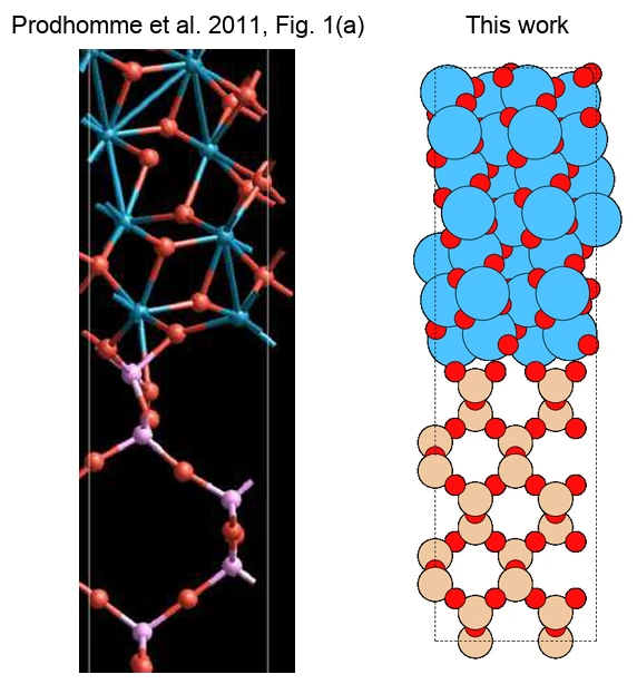
The monoclinic (P2₁/c) superlattice is the model of Prodhomme et al.: ten SiO₂ layers (one Si each) and seven HfO₂ layers (two Hf each), Hf₁₄Si₁₀O₄₈, with three O between the last Si and the first Hf at each interface. The manuscript stretches HfO₂ by 3.7 % along [100] and 2.1 % along [010] from its own lattice; here the strain follows from the lattices of the Standata structures.
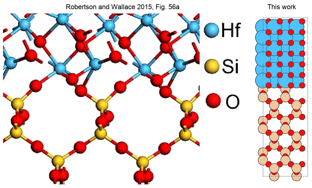
The cubic (Fm-3m) superlattice is the model of Robertson and Wallace, built after Sharia et al. 3: twelve SiO₂ and six HfO₂ layers, Hf₁₂Si₁₂O₄₈. Each interface plane carries three O, two bonded to Si and Hf and one to Hf only, so no Si–O bond is broken.
At each interface the two blocks are separated so that the closest cation–O pair across it is at the bulk bond length of the cation's own oxide. Both manuscripts relax the atomic positions afterwards, as the SiO2/HfO2 (001) Valence Band Offset tutorial does before it computes the offsets. The offsets need, besides the superlattices, bulk cells with the same in-plane lattice, so the notebook saves five materials, which that tutorial loads by name.
2. Open the notebook
2.1. Load the base materials
The notebook loads β-cristobalite SiO₂ (mp-8352), monoclinic HfO₂ (mp-352) and cubic HfO₂ (mp-550893) from Standata, so no input material needs to be selected.
2.2. Launch JupyterLite session
Select the "Advanced > JupyterLite Transformation" menu item to launch the JupyterLite environment, or use the notebook embedded in Section 6.
2.3. Open interface_3d_3d_silicon_dioxide_hafnium_dioxide.ipynb notebook
Find and open interface_3d_3d_silicon_dioxide_hafnium_dioxide.ipynb in the specific_examples folder.
3. Configure and create the structure
3.1. Set parameters
Cell 1.1 of the notebook sets the materials, the Miller indices and layer counts of each block, the atoms removed from the monoclinic HfO₂ block, the in-plane shift of the cubic HfO₂ block, the matching tolerance, and the names of the saved materials:
1 2 3 4 5 6 7 8 9 10 11 12 13 14 15 16 17 18 19 20 21 22 23 24 25 26 | |
3.2. Run the notebook
Execute the notebook by selecting "Run" > "Run All Cells" from the JupyterLite menu.
3.3. Follow the construction
The notebook builds the two superlattices and their bulk cells in five steps:
- The SiO₂ slab is cut from the primitive cell of β-cristobalite, where the Miller indices (1, 1, 0) select the cubic (001) face in the 45° cell, and each HfO₂ slab along (001) from its conventional cell, both without vacuum. The interface builder strains HfO₂ onto the SiO₂ cell. It re-creates its slabs from the bulk, so layer counts and atoms are changed on the built superlattice.
- Monoclinic HfO₂ (section 2): the slab builder counts monoclinic (001) layers in pairs, so eight HfO₂ layers are built and one is removed, the lowest O and the top five atoms. The block kept ends in one O against the SiO₂ O plane and in three O against the SiO₂ Si, so each interface carries three O and the cell stays stoichiometric. The in-plane registry of the two blocks is the builder's default; the manuscript does not give it.
- Cubic HfO₂ (section 3): the HfO₂ block is shifted in plane by a quarter of the cell, so that the interface O of SiO₂ sit on O sites of HfO₂. As built, one interface plane is an HfO₂ O plane with four O and the other the SiO₂ O plane with two. The first O of the four-O plane that is not bonded to Si is removed, and an O is added at the same in-plane position in the two-O plane. Sharia et al. reach the same structure by removing a different O from each of two four-O interface planes.
- In both superlattices, the HfO₂ block is moved along the normal, and the cell length set, so that the closest cation–O pair across each interface is at the bulk bond length: Si–O of SiO₂, Hf–O of the HfO₂ phase.
- Section 4 cuts the bulk reference cells. SiO₂ is used as is, one β-cristobalite period along [001] in the 45° cell; each HfO₂ is strained in plane to the cell of its superlattice, with the (001) layer spacing kept. Atom labels are removed from all five materials, because labels break the Quantum ESPRESSO input.
4. Analyze the structure
Section 5 of the notebook draws the five materials, seen along b with c vertical and repeated twice along a and b; the dotted box outlines the two cells along a. In each superlattice the SiO₂ block is at the bottom of the cell and the HfO₂ block on top; the second interface is across the periodic boundary.
The monoclinic superlattice, Hf₁₄Si₁₀O₄₈, 72 atoms, beside the O-rich SiO₂/HfO₂ interface of Prodhomme et al.:
The cubic superlattice, Hf₁₂Si₁₂O₄₈, 72 atoms, beside the relaxed SiO₂:HfO₂ interface of Robertson and Wallace:
5. Save the structure
Section 6 of the notebook sends the five materials to the environment. In JupyterLite they are passed to Materials
Designer, where they can be saved on the platform; in a local Jupyter session they are written to the uploads
folder, from which the simulation tutorial loads
them.
6. Interactive JupyterLite notebook
The following JupyterLite notebook creates the two superlattices and the three bulk cells. Select "Run" > "Run All Cells".
7. References
-
Pierre-Yves Prodhomme, Fabien Fontaine-Vive, Abram Van Der Geest, Philippe Blaise, and Jacky Even. Ab initio calculation of effective work functions for a TiN/HfO2/SiO2/Si transistor stack. Applied Physics Letters, 99:022101, 2011. URL: https://doi.org/10.1063/1.3609869. ↩
-
John Robertson and Robert M. Wallace. High-K materials and metal gates for CMOS applications. Materials Science and Engineering: R: Reports, 88:1–41, 2015. URL: https://doi.org/10.1016/j.mser.2014.11.001. ↩
-
Onise Sharia, Alexander A. Demkov, Gennadi Bersuker, and Byoung Hun Lee. Theoretical study of the insulator/insulator interface: band alignment at the SiO2/HfO2 junction. Physical Review B, 75:035306, 2007. URL: https://link.aps.org/doi/10.1103/PhysRevB.75.035306. ↩